Assembly

Overview
The MultiGeiger project is an idea by the Ecocurious initiative. The open-source MultiGeiger device for measuring gamma radiation is being developed by the community. Real-time data from stationary units is transmitted via LoRaWAN or WiFi to a server and visualized on a map. This builds a citizen-operated radiation monitoring network. You are warmly invited to join!
Parts
Sort the electronics parts first (see the bill of materials) and check for completeness.
ID(s) |
# |
Picture |
Part |
|---|---|---|---|
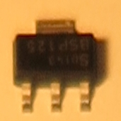
T1 |
1 |
|
BSP125 N-MOS transistor |
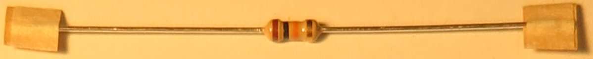
R1 |
1 |
|
10K resistor (brown-black-orange-gold) |
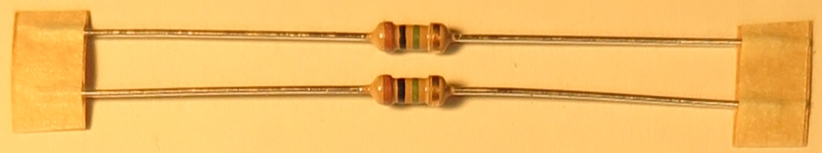
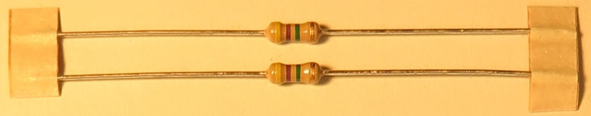
R2 R5 |
2 |
|
1.0M resistor (brown-black-green-gold) |
R3 R4 |
2 |
|
4.7M resistor (yellow-violet-green-gold) |
D1 D2 |
2 |
|
Zener diode ZY 200 |
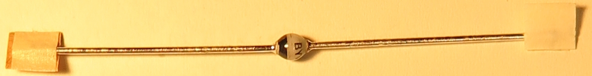
D3 |
1 |
|
Zener diode BZX55C3V3 |
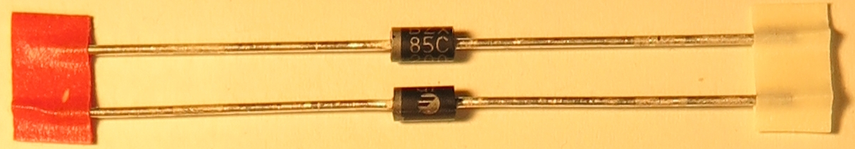
D4 |
1 |
|
Rectifier diode BYV 26E |
D6 |
1 |
|
Rectifier diode GP10Y |
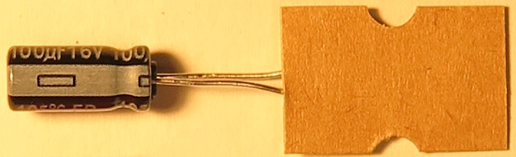
C1 |
1 |
|
Electrolytic capacitor 100 uF, 16 V |
C2 |
1 |
|
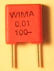
Film capacitor 10 nF, 100 V (0.01 100-) |
C3 |
1 |
|
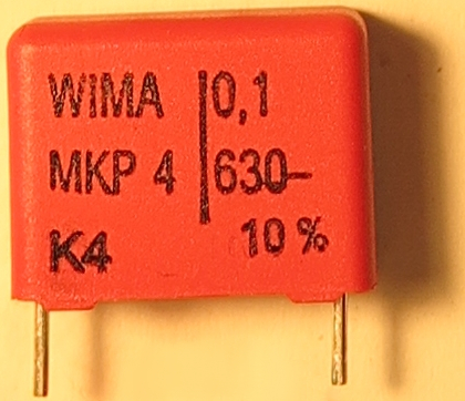
Film capacitor 100 nF, 630 V (0.1 630-) |
C4 |
1 |
|
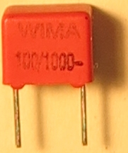
Film capacitor 100 pF, 1000 V (100/1000-) |
L1 |
1 |
|
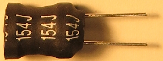
150 mH inductor 154J |
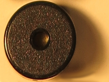
Pz1 |
1 |
|
Piezo speaker |
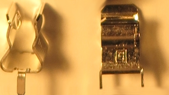
X1 X2 |
2 |
|
Geiger tube holder |
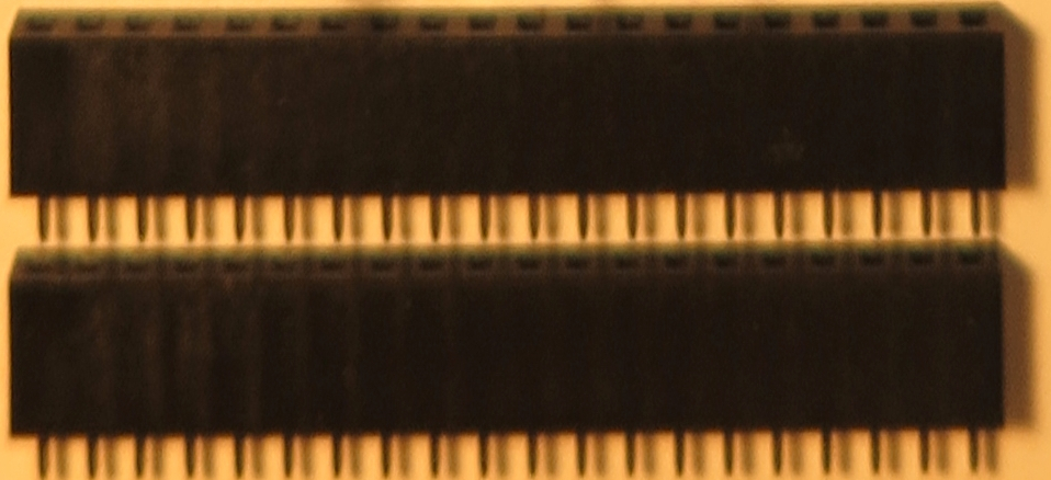
2 |
|
Female header for microcontroller module |
|
2 |
|
30 cm insulated copper wire (each) |
|
1 |
Micro-USB power supply |


Soldering Work
Field-effect transistor T1
Start with the only SMD part on the board. Fix it to the PCB with masking tape so the three pins remain visible. Solder the front pins first, remove the tape carefully, then solder the rear pin.
Resistors and diodes
Bend all resistors and diodes with a bending tool (or gently by hand/small pliers). The width is always four grid units (about 10 mm).
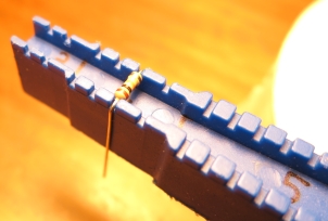
Populate the PCB with the resistors and diodes. Mind diode polarity: the cathode (negative) is marked with a stripe on both PCB and part.
Before soldering on the bottom side, fix the parts on the top with masking tape or slightly bend the leads outward to hold them. Then solder the parts, remove the tape, and trim excess leads.
Note
Risk of injury: take care that clipped leads cannot hit anyone. Hold the lead while cutting.
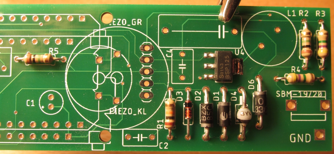
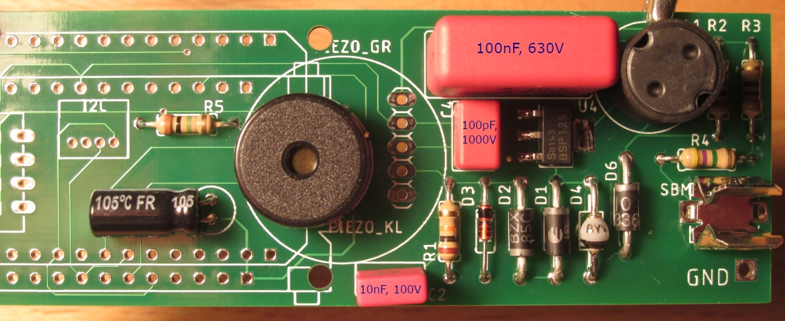
Capacitors and remaining parts
Pre-bend the electrolytic capacitor leads with flat-nose pliers and double-check polarity:
the - pin is marked on the capacitor, the + pad on the PCB. Marks must face each other.
Insert the tube holder so the Geiger tube points outward - test-fit to be sure.
Fix the parts with masking tape, solder, and trim the leads.
Capacitors, tube holder, inductor, and piezo installed:
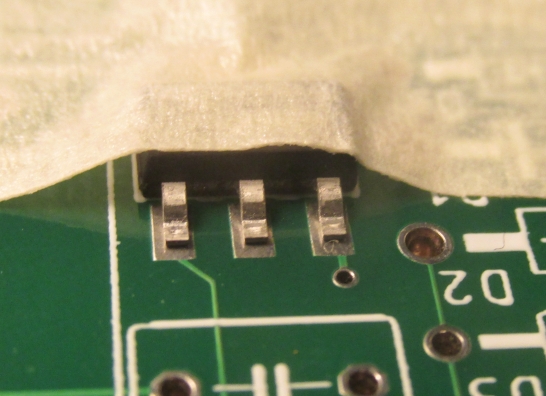
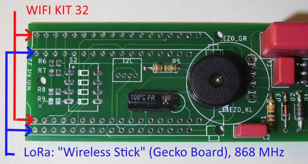
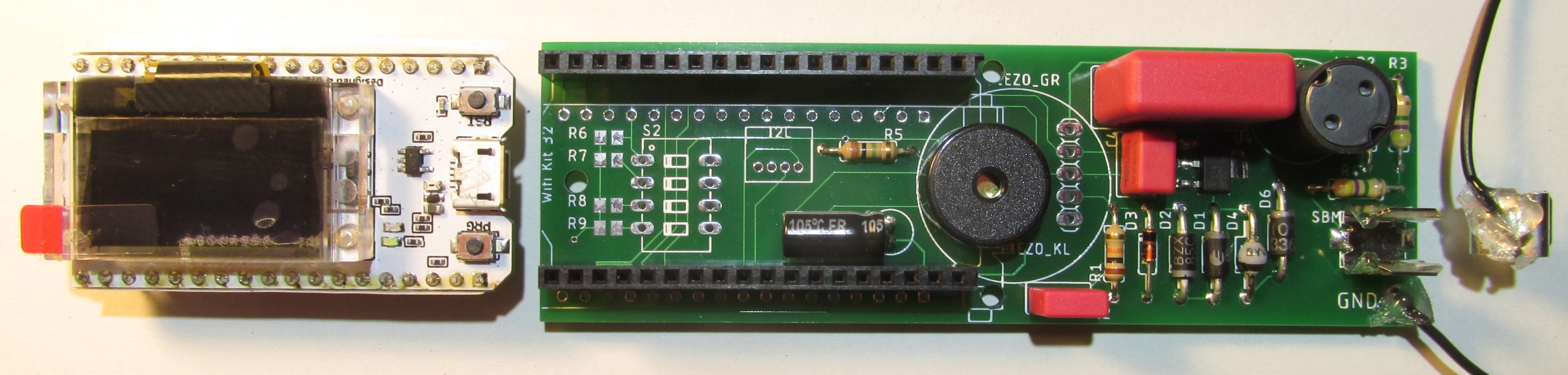
Headers and microcontroller module
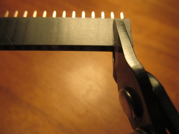
Shorten the female headers if needed.
Note
When cutting, place the side cutter on the last unneeded contact - not at the desired length - otherwise the plastic can split. Hold on to any pieces that may fly away.
If you use the large piezo speaker, file the header slightly so everything fits (test first). The easiest place to file is the original, uncut edge of the header strip. Populate the header positions that match your microcontroller board.
Header angles should be precise. A reliable approach:
Insert the first header.
From the bottom, solder one joint in the middle, reheat it, and align the header (right angle, all pins straight).
Insert the second header.
Plug the long pin headers from the microcontroller kit into both female headers so the long side sits in the female header.
Mount the microcontroller module so the display is visible and the micro-USB socket is above the piezo speaker.
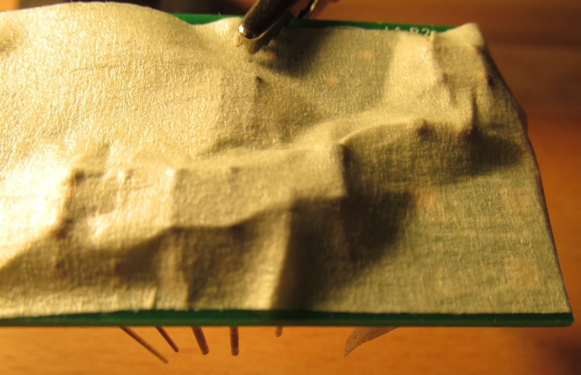
Fix everything with narrow masking tape (see photo) while keeping all joints accessible.
Solder all contacts.
Note
The OLED display is attached via a thin flex cable that must not overheat. If in doubt, skip soldering pins near the flex cable - they are not needed.
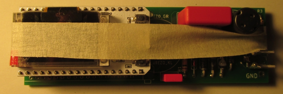
After soldering, carefully remove the microcontroller module with a rocking motion.
Use the pin label stickers that come with the module; apply them to the sides. Pin mapping is printed on the bottom of the board.
Solder the cable for the Geiger tube cathode (negative) to the clip and PCB.
Secure cables with a drop of hot glue for strain relief.
Visual inspection: check for missing joints or solder bridges.
Reattach the microcontroller module.
Connect the Geiger tube; the positive pin (anode) is marked and must face the PCB.
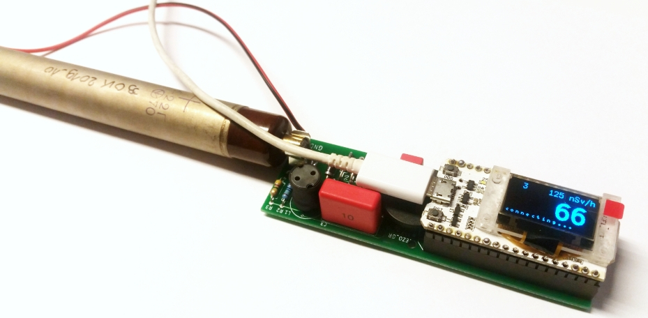
You can now perform a first functional test; see Usage.
Finished Geiger counter and microcontroller board:
Note
The thin glass of the OLED is fragile. Avoid pressing on the display - apply force only to the microcontroller board.
Warning
Danger: the Geiger board generates 400 V. The voltage remains for some time after power-off. Touching it can cause small shocks - usually harmless but should be avoided.

Discharge the capacitor before working on the circuit. The simplest way is to short anode and cathode of the tube for about one second with a second cable (~30 cm). This prevents unpleasant shocks and protects the circuitry.
Optional: I2C interface
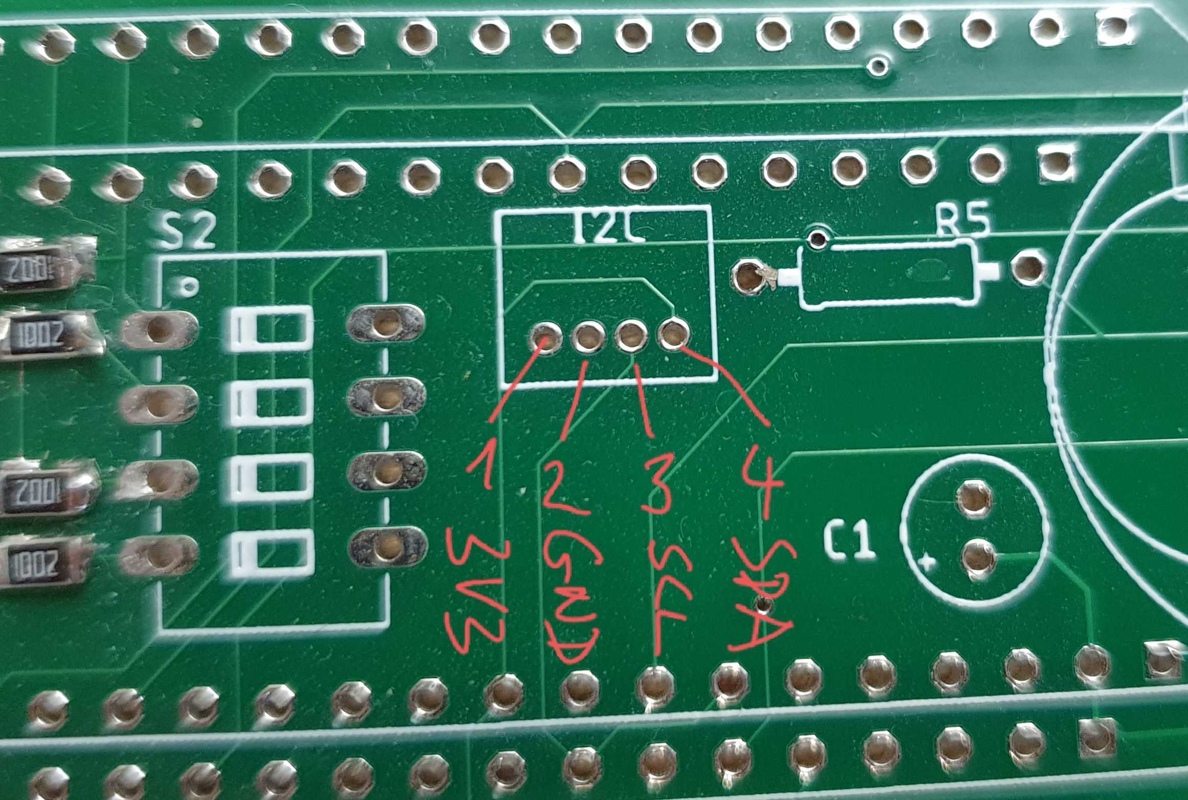
You can add sensors via the I2C interface.
# |
Label |
Description |
|---|---|---|
1 |
3V3 |
3.3 V supply |
2 |
GND |
Ground |
3 |
SCL |
I2C clock |
4 |
SDA |
I2C data |
Currently supported:
Bosch BME280: temperature (C), relative humidity (%), pressure (Pa)
Bosch BME680: temperature (C), relative humidity (%), pressure (Pa), Indoor Air Quality (IAQ) index (25 good .. 500 poor)
Enclosure
Purpose of the enclosure
Protects electronics from weather (rain) and insects (no openings larger than 0.5 mm).
Holds the Geiger tube 1 m above ground so measurements are comparable to the official ODL network.
PVC tubes
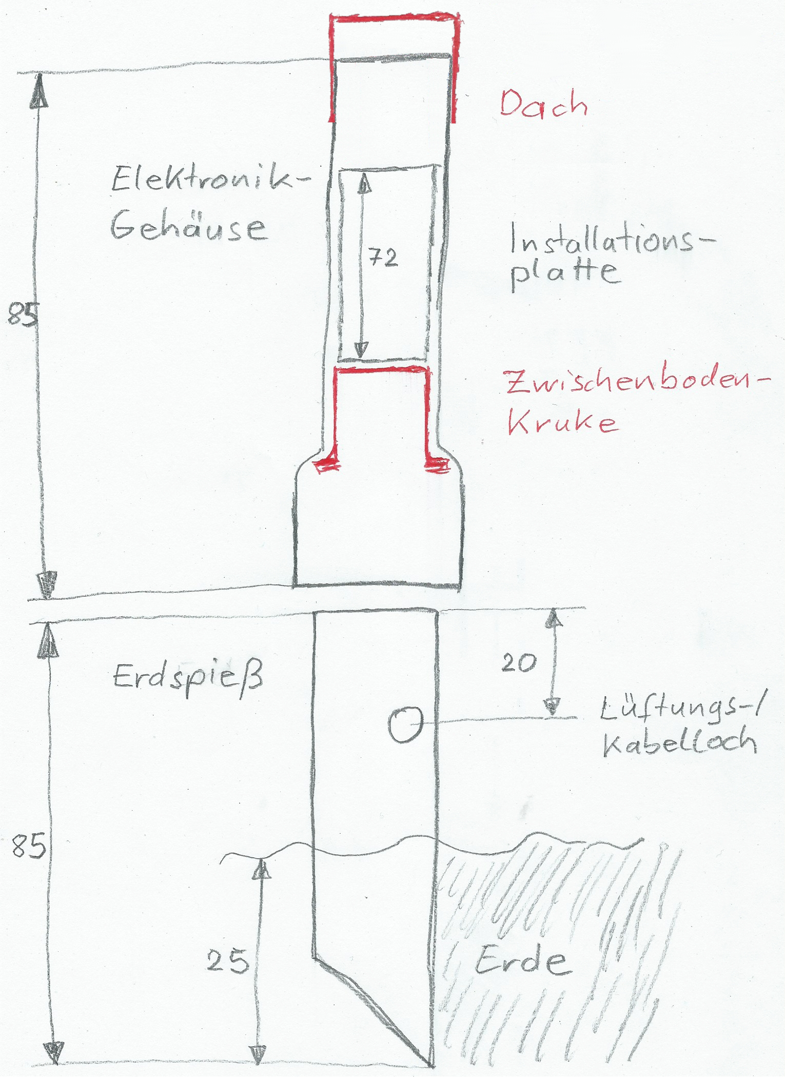
Electronics tube: cut the tube to length with a saw; the socket (widened end) points downward.
Ground spike tube: the remaining piece becomes the top of the ground spike. Cut the bottom at a 45-degree angle to length. The angled tip makes it easier to twist into the ground. Alternatively, keep this piece short (~15 cm) and clamp it into a galvanized parasol ground spike (40 mm inner diameter).
Drill the ventilation/cable hole: pre-punch the hole on the side of the ground spike with a push pin, enlarge it, then use a large drill/step drill to about 17 mm diameter.
Note
Risk of injury: always cut or drill away from your body.
Cap and intermediate floor
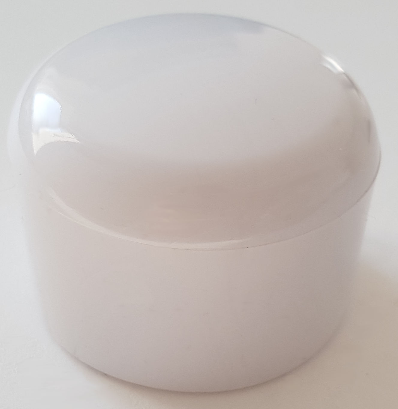
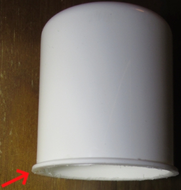
A PVC end cap can be slid over the tube as a roof (see photo).
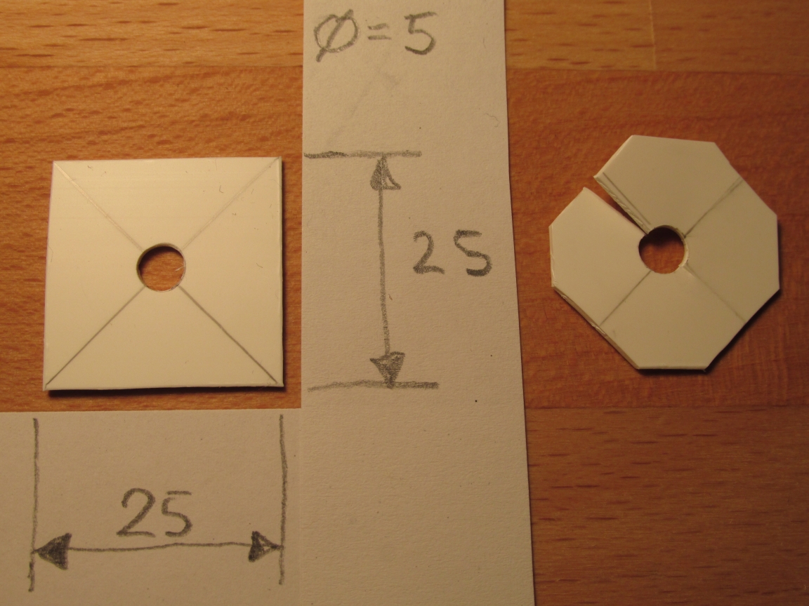
We use a small pharmacy jar as the intermediate floor. Its red lid can be used as the insert that reduces the cable opening.
Saw off only the thread of the jar (see photo); keep the collar because it serves as a stop.
Drill a 10 mm hole in the center of the intermediate floor for cable routing. The plug of the cable must fit through the hole.
An intermediate-floor insert keeps insects out by narrowing the cable opening. You can use the jar lid or a similar piece of plastic.
Mark the center, drill a hole the size of the power cable (~5 mm), then cut off the corners. Add a slit from the outside to the hole.
Intermediate-floor insert (built in two steps):
Mounting plate
The mounting plate can be made from the top or bottom of a cable duct. Carefully cut off the side walls with a knife. Trim the resulting flexible strip to length using strong scissors.
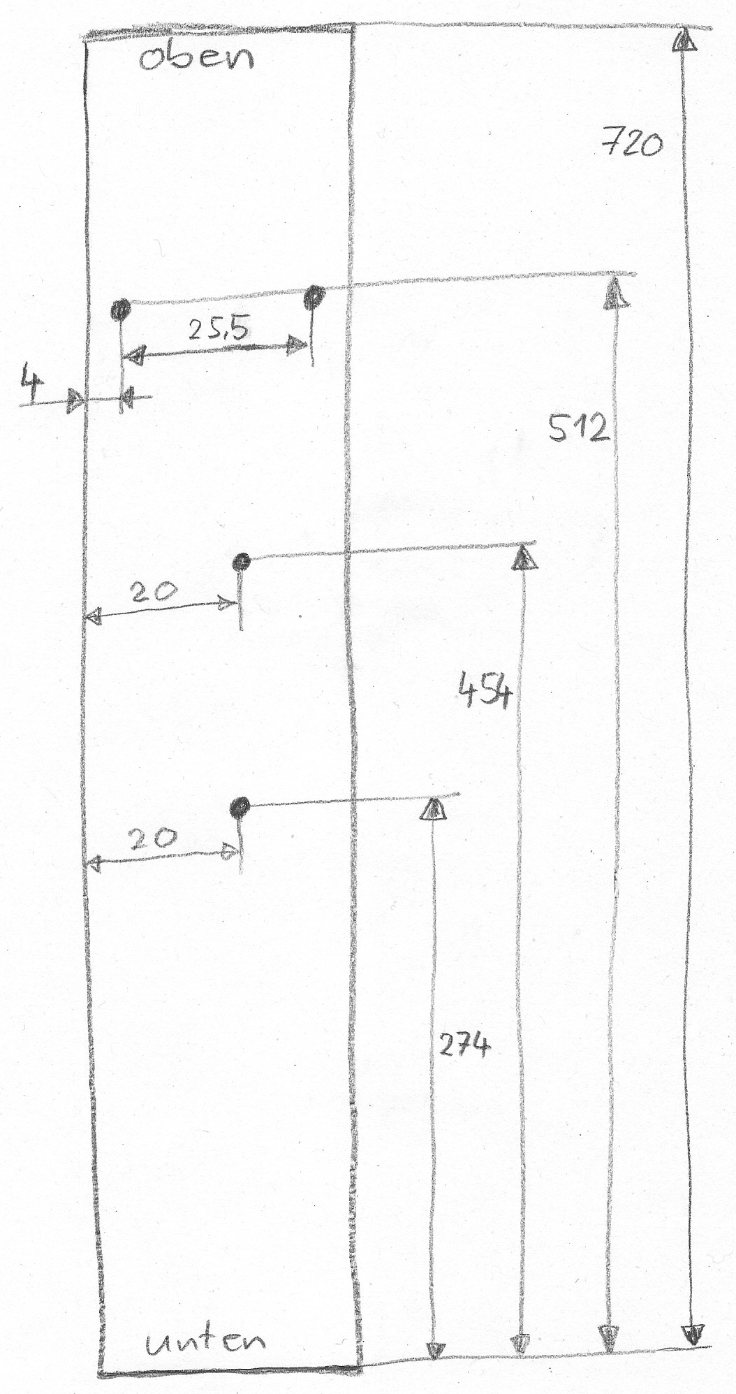
Drill holes through the plate: the electronics and tube are fixed with cable ties so the tube sits at 1 m height when the ground spike is 25 cm in the soil. The tube points downward. Pre-punch the holes with a pin, then drill to 3 mm (see the drilling template).
Mount the PCB with a single cable tie through both holes; it runs below the USB connector.
Drilling template for the mounting plate:
Final assembly
Device assembly (red arrows indicate cable ties):
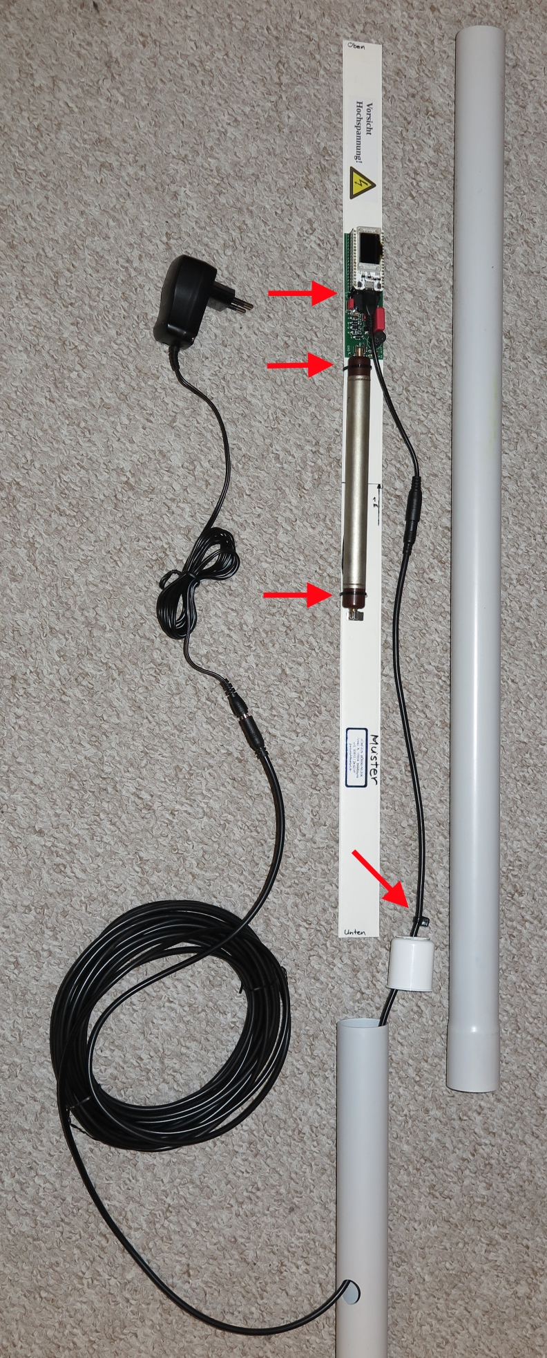
Fix PCB and tube to the mounting plate with cable ties.
Plug the matching adapter into the micro-USB socket.
Thread the 10 m extension cable through the ground spike and intermediate floor in the correct direction, then connect it to the adapter.
Slide the intermediate-floor insert over the cable above the intermediate floor.
Add a cable tie above the insert for strain relief.
First test-fit: slide the mounting plate into the electronics tube, then add the intermediate floor and ground spike.
If everything fits, glue the intermediate-floor insert onto the intermediate floor with silicone and hold with masking tape until cured.
Apply the “High Voltage” warning sticker to the mounting plate.
Commissioning
WiFi variant: the device starts its own WiFi access point (AP).
The SSID is ESP32-xxxxxxxx where xxxx is the WiFi chip ID (example: ESP32-51564452).
Write down this number; it is needed later for registration (e.g., at https://devices.sensor.community/).
The AP stays active for 30 s. Then the device tries to connect to the configured WiFi for 30 s.
If that fails, it returns to AP mode.
The default WiFi password is ESP32Geiger and should be changed soon.
More information: Deployment and Usage.
Enjoy your new device - and may it never detect dangerous spikes!